

Indexed In
- Open J Gate
- Genamics JournalSeek
- Smithers Rapra
- RefSeek
- Directory of Research Journal Indexing (DRJI)
- Hamdard University
- EBSCO A-Z
- OCLC- WorldCat
- Scholarsteer
- Publons
- Geneva Foundation for Medical Education and Research
- Google Scholar
Useful Links
Share This Page
Journal Flyer
Open Access Journals
- Agri and Aquaculture
- Biochemistry
- Bioinformatics & Systems Biology
- Business & Management
- Chemistry
- Clinical Sciences
- Engineering
- Food & Nutrition
- General Science
- Genetics & Molecular Biology
- Immunology & Microbiology
- Medical Sciences
- Neuroscience & Psychology
- Nursing & Health Care
- Pharmaceutical Sciences
Research Article - (2017) Volume 7, Issue 1
Room Temperature Synthesis of Nanocubic CuInSe2 Thin Films
Abstract
The arrested precipitation technique (APT) is used to deposit CuInSe2 thin films. The deposition of thin films is carried out at room temperature. The optical study reveals direct allowed type of transition for CuInSe2 thin films. The XRD pattern confirms mixed phase of CuInSe2 thin films. The SEM image reveals nanocubic thin film formation. The EDS analysis confirms presence of copper, indium and selenium elements in the synthesized thin film. The synthesized thin films are beneficial for the solar cell applications.
Keywords: APT; CuInSe2; Thin films
Introduction
Development of new materials is the major driving force of the technological evolution. During the last two decades immense progress has been achieved in the fabrication and manipulation of nanoscale crystallites and manipulation of the nanoscale crystallites and understanding of the size and shape dependent properties of the nanomaterial’s [1,2].
Taking this fact into consideration, CIS based chalcopyrite thin films have found potential interest in the field of solar energy due to its absorbing property. The CuInSe2 thin films possess characteristic properties such as high absorption coefficient, tunable band gap and high stability. Among the I-III-VI ternary chalcopyrite’s CuInSe2 thin films have a calculated exciton Bohr radius of approximately 10.6 nm and have a lowest band gap of 1.04 eV with largest absorption coefficient. It has less toxicity than other semiconductor nanomaterial’s currently being used [3-6].
The electronic structure of these materials strongly relate with the [Cu]/[In] ratios there is a great need to precisely control their size, shape, surface and composition. Nowadays, great success has been achieved in the synthesis of ternary, quaternary nanomaterials via several routes. The methods for the synthesis are solvothermal approach, hot injection method, thermal decomposition, chemical bath deposition, electrode position etc. [7-11].
Considering all these facts we are reporting here a low cost arrested precipitation technique for the deposition of CuInSe2 thin films. Further the optical, structural, morphological and compositional properties of CuInSe2 thin films have been investigated.
Materials And Methods
All the chemicals were analytical reagent (AR) grade and used without further purification. The list of chemicals used to deposit CuInSe2 thin films is given in Table 1. Herein the depositions of CuInSe2 thin films were carried out onto glass substrates as well as FTO using APT at room temperature.
| Chemicals | Chemical formula | Company |
|---|---|---|
| Copper sulphate (99.5%) | CuSO4·5H2O | SD-fine Chem limited |
| Indium sulphate (99.9%) | In2(SO4)3 | Spectrochem |
| Triethanolammine (99.0%) | N(CH2-CH2-OH)3 | Merck |
| Liquor ammonia (28-30 %) | NH3 | Thomas Baker |
| Selenium metal powder (99.5%) | Se | Sigma Aldrich |
| Sodiumsulphite anhydrous (96.0%): | Na2SO3 | SD-fine Chem limited |
Table 1: Chemicals used to deposit CuInSe2 thin films.
Deposition of CuInSe2 thin films
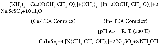
The 0.05 M Cu-TEA and 0.05 M In-TEA complexes were used as a source of Cu2+ and In3+ ions respectively. They were prepared by dissolving the [CuSO4.5H2O] and In2(SO4)3 salts separately with TEA complexing agent. A 0.25 M Na2SeSO3 solution was prepared by dissolving 99% pure selenium metal powder in saturated solution of Na2SO3 by refluxing the whole solution for 8 h at 60°C and used as a source of Se2− ions. In order to deposit CuInSe2 thin films an 8 mL of 0.05 M Cu-TEA and 2 mL of 0.05 M In-TEA complex solutions were taken in reaction bath container. The pH of the reaction mixture was adjusted to 9.5±0.5 by drop wise addition of aqueous ammonia. Then 10 mL of 0.25 M Na2SeSO3 solution was added to the reaction mixture with constant stirring. The total volume of reaction bath was made to 40 ml by adding double distilled water. The reaction mixture was stirred for 10 minutes on a magnetic stirrer to get homogeneous solution. The precleaned glass substrates were immersed vertically in the reaction bath and then kept at room temperature without stirring for 3 hrs. When the terminal growth is over films withdrawn from reaction bath and designated as CuInSe2. In detailed optimized parameters are given in Table 2.
| Sample | Optimized preparative parameters | |||
|---|---|---|---|---|
| Bath composition | pH | Temperature (K) | Deposition time (h) | |
| CuInSe2 | 5.0 ml 0.05 M Cu -TEA complex solution+2ml 0.05 M In-TEA complex solution+10ml 0.25 M Na2SeSO3 solution, total volume made to 40 ml by adding double distilled water | 9.5 ± 0.5 | Room temperature (300 K) | 3 |
Table 2: Optimized preparative parameters for the deposition of CuInSe2 thin films.
Characterizations of CuInSe2 thin films
The synthesized thin films were characterized for their thickness, optical, structural, morphological, compositional properties. Thickness of the films was measured by using Ambios XP-1 surface profiler. The absorption spectrum was recorded in the range of 400-1100 nm by using a UV-Vis-NIR spectrophotometer (Shimadzu UV-1800). XRD patterns were obtained using X-ray diffractometer (Bruker AXS Model D8 Advance) in the 2θ range 20-80° with Cu Kα as a target.
The surface morphology of films was studied using scanning electron microscopy (SEM-S-4700, Hitachi). Chemical compositions of synthesized thin films were studied by energy dispersive X-ray spectroscopy (EDS) technique attached to SEM equipment.
Results And Discussion
Growth and reaction mechanism of CuInSe2 thin films
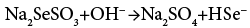
The controlled and slow release of ions is the main beauty of APT. Hence we have used a TEA as complexing agent. The Na2SeSO3 solution added to the cationic alkaline reaction mixture play dual role as a source of Se2− ions as well as a reducing agent due to presence of excess Na2SO3. At alkaline pH, Na2SeSO3 hydrolyses into Na2SO4, follows base catalyzed reaction and release Se2− ions into the solution as per the reactions (1) and (2)
 (1)
(1)
 (2)
(2)
The excess Na2SO3 oxidises into Na2SO4 and releases electrons concomitantly, which are responsible for the reduction of Cu+2 into Cu+1 states during the deposition of CuInSe2 and according to reactions (3) and (4)
 (3)
(3)
 (4)
(4)
The APT is based on the principle of Ostwald ripening law. Initially, there is a formation of seed nuclei take place. These nucleation centres form a monolayer on a substrate by ion by ion condensation. The number of smaller crystallites comes together to form a larger crystallites in accordance with the Ostwald ripening law.
Following chemical reactions (5) and (6) are proposed for the formation of CuInSe2 thin films in this investigation:
Optical study
The absorption spectra of CuInSe2 thin films are recorded in the range of 300 nm to 1100 nm on a UV-Vis spectrophotometer. The absorption spectra and band gap is shown in the Figure 1. The absorption is in the visible range of solar spectrum. The band gap of a thin film is determined by using the following equation,
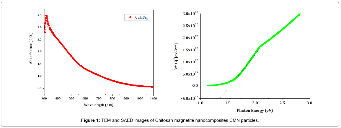
Figure 1: TEM and SAED images of Chitosan magnetite nanocomposites CMN particles.
 (7)
(7)
Where, ‘h’ is Planck’s constant, ‘Eg’ is Band gap of the material, ‘A’ is Parameter depends on the transition probability, ‘n’ is exponent. Exponent ‘n’ may have values such as 1/2, 3/2, 2 and 3 depending on the nature of electronic transition responsible for the absorption of light. The value of n=1/2 for allowed and direct transition, n=3/2 for direct forbidden transition n=2 for indirect allowed transition, n=3 for indirect forbidden transition. The nature of obtained data confirms that CuInSe2 thin films shows a direct allowed type of transition with a band gap 1.38 eV. Such a band gap is highly beneficial for the solar cell applications.
Structural study
XRD spectra of CuInSe2 thin films show the peaks of CuInSe2 with mixed phases of Cu2Se3 and In2Se3 phases. The XRD pattern of CuInSe2 thin film is shown in Figure 2. The observed peaks corresponding to the (101), (111), (210), (211), (002) and (311) planes are of Cu2Se3 phase, whereas (101), (205), (021) planes in the XRD belong to In2Se3. The peak observed (112), (103), (211), (105), (220), (301), (312), (323) and (316) are corresponds to CuInSe2 (JCPDS file No.81-1936). CuInSe2 have tetragonal crystal structure with lattice constants a=5.781 Å and c=2.0139Å. The crystallite size of CuInSe2 thin film samples calculated from well-known Scherer’s formula.
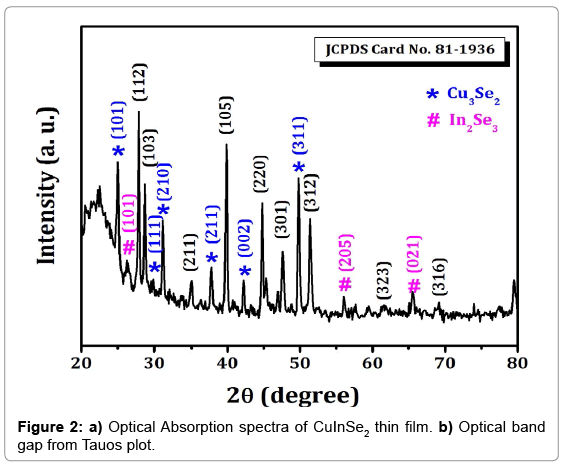
Figure 2: a) Optical Absorption spectra of CuInSe2 thin film. b) Optical band gap from Tauos plot.
From calculated values of crystallite size the dislocation density (δ) and microstrain (ε) for all the samples were determined by using equation 8 and 9 respectively.
 (8)
(8)
 (9)
(9)
Where, D is crystallite size, θ is Bragg’s diffraction angle and β is full width at half maximum (FWHM). The obtained values of (δ) and () of CuInSe2 thin film given in Table 3.
| Sample Code | Crystallite Size (D) nm | Dislocation Density (d) × 10-3 lines/nm2 | Microstrain (e) × 10−3 |
|---|---|---|---|
| CuInSe2 | 60.6 | 2.7149 | 0.1405 |
Table 3: Variation of crystallite size (D), dislocation density (δ) and microstrain (ε) CuInSe2 thin film.
Morphological study
In order to study the morphological aspects of CuInSe2 thin films, FESEM analysis is carried out. The low resolution and high resolution SEM images show a uniform, adherent, pin hole free thin film formation. The SEM images reveal nanocubic structure for thin films. Such a nanocubic structures are interconnected with each other. The interconnected nanocubic structure provides a better pathway for the conduction of electrons. Hence it is beneficial for the solar cell applications. The Figure 3 shows SEM images of CuInSe2 thin films.
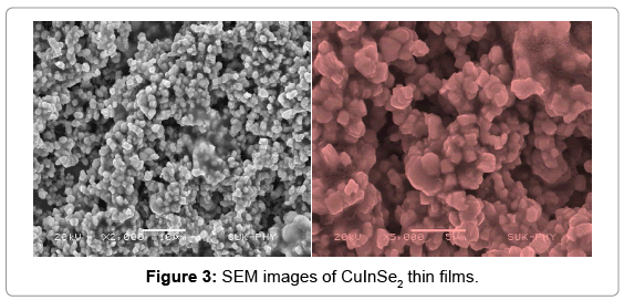
Figure 3: SEM images of CuInSe2 thin films.
Compositional study
The quantitative analysis of CuInSe2 thin films is done using EDS analysis. The EDS spectrum shows a three principle peaks for Cu, In and Se respectively. The observed atomic percentage of CuInSe2 thin films is in well agreement with the expected atomic percentage. Hence the presence of Cu, In and Se in the synthesized thin film is confirmed by EDS. The EDS spectrum is shown in the Figure 4.
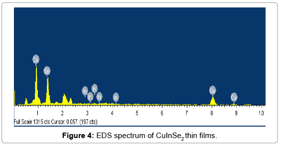
Figure 4: EDS spectrum of CuInSe2 thin films.
Conclusions
The nanostructured CuInSe2 thin films are successfully synthesized by APT at room temperature. The opt structural, morphological, compositional properties of CuInSe2 thin films are studied. The optical study reveals a band gap 1.38 eV. The X-ray diffraction study confirms nano crystalline nature of CuInSe2 thin films. The SEM images reveal uniform nanocubic thin film formation. The presence of Cu, In and Se in the synthesized thin film is also confirmed by EDS. All these parameters reveal that CuInSe2 thin films are beneficial for the solar cell applications.
Summary
Today scientists all over the world are working on the solar cell technology. The chalcopyrite and chalcogenide thin films are considered as potential candidates for the solar cell applications. The chalcopyrite thin films possess characteristic properties such as high absorption coefficient, tunable band gap, high stability etc. Considering all these facts we are interested in the synthesis of CuInSe2 thin films. Here we have used a simple and low cost arrested precipitation technique for the synthesis of CuInSe2 thin films. CuInSe2 thin films is the most widely studied material for their optostructural and optoelectronic properties. Hence, we have done the characterization of CuInSe2 thin films to know their optical, structural, morphological and compositional properties.
References
- Chen G, Wang L, Sheng X, Yang D (2011) Direct synthesis of indium nanoparticles and their application to prepare CuInS2 thin films and solar cells. J Solgel Sci Technol 58: 162-169.
- Wang Y, Rui Y, Zhang Q, Li Y, Wang H (2013) A Facile in Situ Synthesis Route for CuInS2 Quantum-Dots/In2S3 Co-Sensitized Photoanodes with High Photoelectric Performance. ACS Applied Materials and Interfaces 5: 11858-11864.
- Kolnay-Olesiak J, Weller H (2013) Synthesis and Application of Colloidal CuInS2 Semiconductor Nanocrystals. ACS Applied Materials and Interfaces 5: 12221-12237.
- Lugo S, Lopez I, Pena Y, Calixato M, Hernandez T, et al. (2014) Thin Solid Films 569: 76-80.
- Yaw J, Chang SC, Tzing S, Li C (2014) ACS Applied Materials and Interfaces 6: 22272-22281.
- Hui Liua ZJ, Xin W, Xuerong Z, Yueqiu W, Haiyan D, et al. (2012) Morphological growth and phase formation of CuInSe2 nanocrystals by an ambient pressure polylol-based solution synthesis. CrystEngComm 14: 8186-8192.
- Meadows HJ, Misra S, Simonds BJ, Kurihara M, Schuler T, et al. (2017) J Mater ChemC 5: 1336-1345.
- Hamed A, Yi H, Christoph JB (2014) Towards low-cost, environmentally friendly printed chalcopyrite and kesterite solar cells. Energy Envi Sci 7: 1829-1849.
- Tomoaki T, Yuji U, Tetsuya K, Sho S (2006) Solar Energy Materials and Solar Cells 90: 262-275.
- Marianna K, Mikko R, Markku L (2001) Effects of post-deposition treatments onthe photoactivity of CuInSe2 thin films deposited by the inducedco-deposition mechanism. J Mater Chem 11: 668-672.
- Wentuan B, Min Z, Zhengyu M, Hanyang Z, Jiabing Y, et al. (2012) CuInSe2 ultrathin nanoplatelets: novel self-sacrificial template-directed synthesis and application for flexible photodetectors. Chem Commun 48: 9162-9164.
Copyright: © 2017 Vidya Patil S, et al. This is an open-access article distributed under the terms of the Creative Commons Attribution License, which permits unrestricted use, distribution, and reproduction in any medium, provided the original author and source are credited.