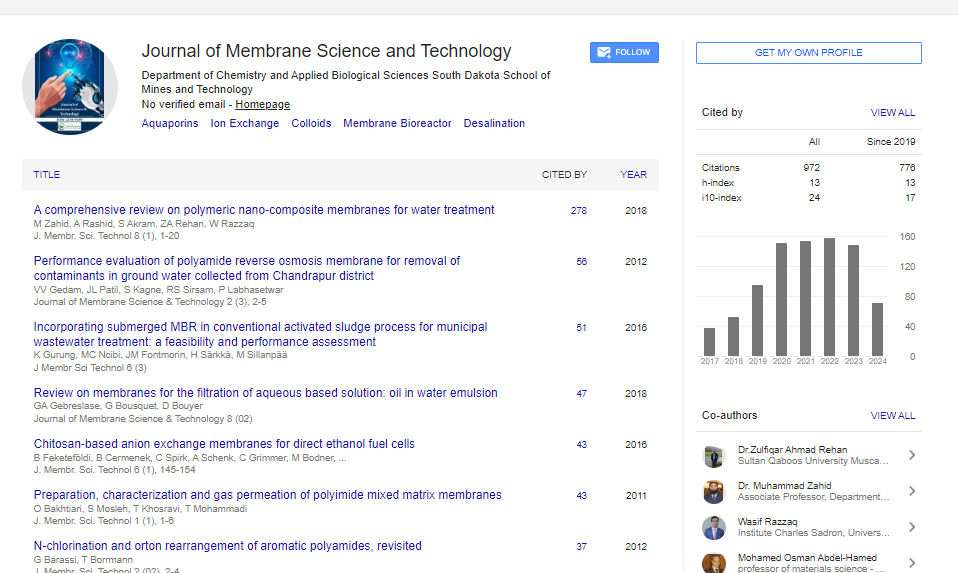

Indexed In
- Open J Gate
- Genamics JournalSeek
- Ulrich's Periodicals Directory
- RefSeek
- Directory of Research Journal Indexing (DRJI)
- Hamdard University
- EBSCO A-Z
- OCLC- WorldCat
- Proquest Summons
- Scholarsteer
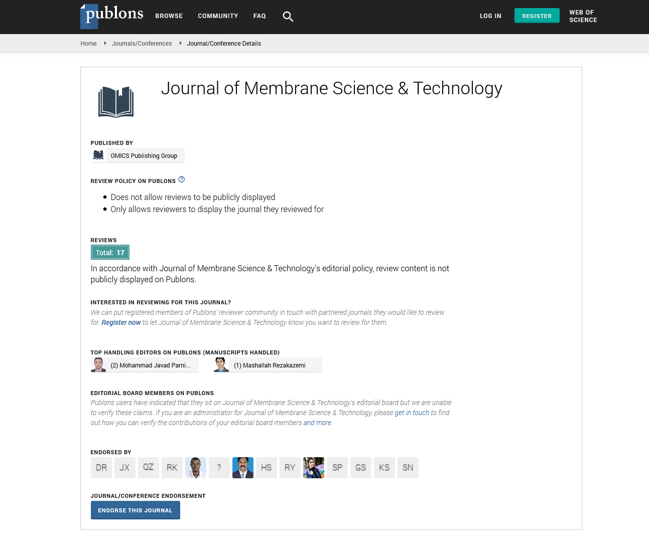
- Publons
- Geneva Foundation for Medical Education and Research
- Euro Pub
- Google Scholar
Useful Links
Share This Page
Journal Flyer
Open Access Journals
- Agri and Aquaculture
- Biochemistry
- Bioinformatics & Systems Biology
- Business & Management
- Chemistry
- Clinical Sciences
- Engineering
- Food & Nutrition
- General Science
- Genetics & Molecular Biology
- Immunology & Microbiology
- Medical Sciences
- Neuroscience & Psychology
- Nursing & Health Care
- Pharmaceutical Sciences
Short Communication - (2022) Volume 12, Issue 12
Basic Experiments and Prospects of Atomic Layer Deposition for Membranes
Guy Segal-Peretz*Received: 29-Nov-2022, Manuscript No. JMST-22-19458; Editor assigned: 02-Dec-2022, Pre QC No. JMST-22-19458 (PQ); Reviewed: 16-Dec-2022, QC No. JMST-22-19458; Revised: 23-Dec-2022, Manuscript No. JMST-22-19458 (R); Published: 30-Dec-2022, DOI: 10.35248/2155-9589.22.12.317
Description
Atomic Layer Deposition (ALD) is a gas-phase deposition method that uses successive surface reactions to create thin films of various materials. The target substrate is subjected to each successive reaction before being exposed to the next, as is the case with other gas phase deposition methods [1]. Only a monolayer of a particular precursor reacts with or chemisorbs on the surface of these surface-limited reactions. In comparison to other thin film deposition techniques, such as Chemical Vapor Deposition (CVD) and Physical Vapor Deposition (PVD), the outcome is a conformal coating that is pinhole-free and has higher process control. Key characteristics of ALD include thickness control with atomic layer accuracy and precision, conformal coverage over high aspect ratio and high surface area materials, extremely low defect density with high uniformity, complex and multilayered films (such as nanolaminates, nanoalloys, and precise doping), and a variety of insulating, conducting, and semiconducting films. These features have led to ALD's growing applications in the design and fabrication of advanced materials and devices [2].
On flat surfaces, the ALD of numerous different materials has been demonstrated. Al2O3, ZnOx, InOx, TiO2, ZrO2, SiO2, HfO2, Ta2O5, and SnO2 are examples of oxides. SiNx, TaNx, BN, and TiN are examples of nitrides. Pt, Ni, Ir, Pd, Ru, and Au are examples of pure metals. For ALD of various materials and composites, new procedures are constantly being developed. Not all of these materials, however, could be conveniently applied to materials with high surface areas and high aspect ratio nanopores. Particularly, plasma-based ALD techniques are not well suited since plasma doesn't enter the pores very deeply. Conformal coatings with high aspect ratio nanopores in materials such as AAO, on the other hand, are better suited for thermal ALD processes. Other microelectronic devices, such as hard drives, biomedical components and devices, such as implantable sensors and drug delivery devices, materials for energy generation and storage, and semiconductor manufacturing of advanced microprocessors (gate dielectrics, advanced lithography, and barrier/seed) and memory (capacitor dielectrics) are applications of ALD (i.e., photocatalytic materials, electrodes for batteries, and supercapacitors). Deposition of highly tailored ALD coatings onto high surface area substrates is used in numerous applications, including the production of nanoparticles and nanoporous membranes as well as integrated circuits with complicated topologies and high aspect ratio vias [3].
With precise thickness control, great conformality, and high uniformity, Atomic Layer Deposition (ALD) is a method that can create thin films of high-quality materials on surfaces with high aspect ratios. As a result, this approach is particularly well suited for altering the structural and pore characteristics of synthetic membranes [4]. ALD coatings have been created on a wide range of membrane substrates, including porous polymers and inorganic templated supports. Using a selected set of research, the application of the ALD approach to improve the operational performance of various inorganic, organic, hybrid, or composite membranes will be demonstrated. Additionally, the road to these particular membrane applications' problems and prospects is highlighted. This work thoroughly demonstrates the advantages of ALD and its use in many engineering processes related to membranes and their components, and it will assist in taking advantage of the many opportunities offered by this newly developing and expanding field [5].
Global water stress and difficulties in providing adequate amounts of usable water are worsening. Advanced water treatment materials are being made with the help of atomically designed interfaces, which are becoming an increasingly potent technology. Sequential Infiltration Synthesis (SIS), a recently discovered similar technique, and Atomic Layer Deposition (ALD) provide a hugely varied library of chemicals for interface functionalization. Precision manipulation of thickness, stoichiometry, and physicochemical characteristics is possible. We go into the physical chemistry and processing principles underlying them. With the goal of achieving effective water treatment, ALD/SIS engineering solutions, including direct deposition, growth with intermediate layers, and secondary treatment, are given.
References
- Weber M, Julbe A, Ayral A, Miele P, Bechelany M. Atomic layer deposition for membranes: Basics, challenges, and opportunities. Chem Mat. 2018;30(21):7368-7390.
- Yang HC, Waldman RZ, Chen Z, Darling SB. Atomic layer deposition for membrane interface engineering. Nanoscale. 2018;10(44):20505-20513.
[Crossref] [Google Scholar] [PubMed]
- Xiong S, Qian X, Zhong Z, Wang Y. Atomic layer deposition for membrane modification, functionalization and preparation: A review. J Membr Sci. 2022:120740.
- Xiong G, Elam JW, Feng H, Han CY, Wang HH, Iton LE, et al. Effect of atomic layer deposition coatings on the surface structure of anodic aluminum oxide membranes. J Phys Chem B. 2005;109(29):14059-14063.
[Crossref], [Google Scholar] [PubMed]
- Li F, Yang Y, Fan Y, Xing W, Wang Y. Modification of ceramic membranes for pore structure tailoring: The atomic layer deposition route. J Membr Sci. 2012;397:17-23.
Citation: Peretz GS (2022) Basic Experiments and Prospects of Atomic Layer Deposition for Membranes. J Membr Sci Technol. 12:317.
Copyright: © 2022 Peretz GS. This is an open-access article distributed under the terms of the Creative Commons Attribution License, which permits unrestricted use, distribution, and reproduction in any medium, provided the original author and source are credited.